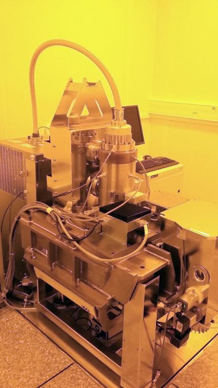
Spot
- Acceleration voltage: 20 kV up to 100 kV (routine use 80kV)
- Probe current: up to 100nA
- Spot size: 3nm
- Current resolution: 20nm but it is theoretically possible to go below 15nm
- Exposure dose control: in real time, with 0.5 Hz increments
Turntable
- Magnification: up to x 300,000
- Laser interferometric controlled plate (positioning accuracy λ/2048 or 0.31 nm)
- Displacement: X 200mm, Y 200mm
Loading
- Automatic sample transfer from the airlock to the plate
- Cassette : 10 chucks
- Chuck: electrostatic and mechanical clamping.
Samples
- Sample sizes: wafers from 2 to 8" (20.3 cm); masks (rectangular) up to 7" (17.8 cm), square samples from 5mm to 20 mm.
- Writing field: up to 800 µm with a resolution of 1nm
- Writing area: 198 mm x 198 mm